Showing posts sorted by date for query GaN. Sort by relevance Show all posts

EIB to invest €90mn in Metlen gallium plant to rebuild Europe’s supply

No comments
EIB to invest €90mn in Metlen gallium plant to rebuild Europe’s supply
Metlen gallium

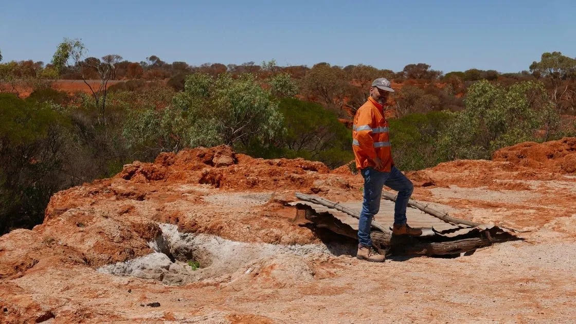
EIB to invest €90mn in Metlen gallium plant as Europe pushes to secure critical minerals. The financing supports a new gallium facility in central Greece. As a result, EIB to invest €90mn in Metlen gallium plant signals faster EU-backed industrial reshoring.

Metlen will modernize bauxite mining and add gallium recovery as a by-product of processing. Meanwhile, the project targets commercial-scale output outside China. EIB to invest €90mn in Metlen gallium plant also strengthens the aluminium value chain in Europe.

Europe restarts gallium production after years of dependence

Europe has lacked commercial-scale gallium production since 2016. Germany and Hungary previously supplied the market from bauxite by-products. However, Europe now relies heavily on imports for semiconductor and defense applications.
China tightened gallium exports in 2023 under new controls. Therefore, buyers faced tighter availability and higher procurement risk. Prices rose sharply as supply flexibility narrowed.

What 50 t/yr gallium means for semiconductors and defense

Metlen plans to reach up to 50 t/yr of gallium by 2028. This volume could cover Europe’s current import needs. As a result, chipmakers and advanced materials users gain a nearer supply option.

Gallium supports high-performance semiconductors such as GaN and other critical technologies. Meanwhile, defense and energy transition demand increases scrutiny on supply security. The project must still execute on ramp-up, recovery yields, and operating stability.

The Metalnomist Commentary

Europe is moving from policy talk to industrial capacity in gallium. However, the market will judge this project on ramp reliability and cost discipline. If Metlen delivers, Europe gains leverage in a tightly controlled metal.

Gallium and scandium extraction facility wins $29.9mn US defence-linked funding

No comments
Gallium and scandium extraction facility wins $29.9mn US defence-linked funding
Critical Minerals

US defence-linked funding will back a gallium and scandium extraction facility at Element USA. The $29.9mn award targets a demonstration site in Gramercy. As a result, the gallium and scandium extraction facility aims to strengthen supply for strategic industries.

Meanwhile, the project also supports early development work at a Critical Resource Accelerator in Cedar Park. The funding uses Defence Production Act funding to scale extraction from industrial waste. Therefore, US onshoring efforts gain another pathway beyond conventional mining.

Turning bauxite residue into strategic metals

Element USA plans to extract gallium and scandium from industrial bauxite residue. The approach targets stockpiled waste that often carries untapped critical minerals. However, commercial success depends on consistent feed quality and reliable separation performance.

The project positions industrial waste as a domestic supply option. It also links alumina by-products to higher-value metals markets. As a result, refiners and waste handlers may see new incentives to collaborate.

Defence demand reshapes critical minerals strategy

Defence platforms rely on gallium and scandium for high-performance applications. Gallium supports advanced GaAs and GaN semiconductors used in radar and secure communications. Meanwhile, scandium strengthens lightweight alloys used in aircraft and missile structures.

The funding also signals sharper competition for specialised grades. Battery supply chains focus on scale and cost. However, defence supply chains prioritise traceability, performance, and resilience. Therefore, projects like this often target strategic availability before mass-market volumes.

The Metalnomist Commentary

This investment treats waste streams as a strategic resource, not a disposal problem. If the plant proves repeatable yields, it can shorten lead times for defence-grade inputs. However, sustained economics will still hinge on offtake confidence and stable residue supply.

STMicro targets new sources of silicon chip demand

No comments
STMicro targets new sources of silicon chip demand
STMicro

STMicro is betting on new sources of silicon chip demand from AI data centres and advanced EV platforms. The company sees silicon and silicon carbide (SiC) devices as core growth engines, even as it trims some near-term capital spending. As a result, STMicro is repositioning its portfolio toward photonics, high-voltage power electronics and next-generation vehicle systems that can unlock new sources of silicon chip demand across several end markets.

Photonics and AI servers anchor new sources of silicon chip demand

STMicro is using silicon photonics to capture new sources of silicon chip demand from hyperscale AI data centres. In the third quarter, the firm reported rising orders for silicon photonics integrated circuit prototypes from its 300mm fabs. This confirms internal expectations that photonics ICs will become a meaningful revenue driver as AI server build-outs accelerate worldwide.

Meanwhile, the company is tightening its integration into the AI infrastructure ecosystem through the Starlight Consortium. The consortium connects substrate suppliers, device makers and system integrators to develop high-speed optical solutions for data centres, telecoms and automotive. In parallel, STMicro is collaborating with Nvidia on an 800V DC AI data centre architecture that combines SiC, gallium nitride (GaN) and silicon technologies. The firm has also demonstrated a GaN prototype with over 98pc conversion efficiency, underscoring how power density and efficiency now drive silicon chip demand as much as raw compute.

SiC, EV power electronics and a more selective capex strategy

STMicro is broadening SiC usage beyond traction inverters and onboard chargers to new power roles in active suspension inverters. This expands the addressable market in EVs just as advanced driver-assistance systems increase demand for sensors and control chips. However, weaker-than-expected EV programmes in Europe and China have delayed the full impact, forcing the company’s main automotive customer to cut orders.

Therefore STMicro is trimming near-term SiC capex as it transitions production from 150mm to 200mm wafers. The company will slow some investments in SiC conversion while maintaining its 300mm expansion plans in Agrate, Italy, and Crolles, France. These fabs continue to see solid order visibility, particularly for data-centre power modules and optical components. STMicro expects EV growth and SiC restocking to resume in 2026, once inventory drawdowns run their course and regional electrification policies translate into firmer demand.

The Metalnomist Commentary

STMicro’s push into photonics and SiC power devices shows how new sources of silicon chip demand are shifting toward AI infrastructure and complex EV systems. For the wider materials chain, this means sustained pull for high-purity silicon, SiC substrates and GaN epitaxy, even if near-term EV softness delays some projects. Suppliers that align with 300mm and 200mm wafer roadmaps and can support AI-class power densities will be best positioned as these new demand waves crystallise from 2026 onward.

IQE GaSb and GaN strategy pivots business toward AI and power markets amid sale options

No comments
IQE GaSb and GaN strategy pivots business toward AI and power markets amid sale options
IQE

IQE’s GaSb and GaN strategy is reshaping the UK compound semiconductor maker as it explores a potential sale of the company. The IQE GaSb and GaN strategy shifts focus toward high-value sensing, photonics and power electronics while legacy wireless markets remain under pressure. As a result, the IQE GaSb and GaN strategy now sits at the core of IQE’s turnaround and M&A narrative.

IQE has continued to rationalise its footprint while redirecting capital to growth nodes. The firm suspended manufacturing at its Silicon site in south Wales and plans to exit fully by the fourth quarter, with a new operator taking over the facility. This follows the sale of its decommissioned Bethlehem, Pennsylvania site in late 2023, with skills, IP and customers transferred to Greensboro, North Carolina. That larger US site now anchors IQE’s presence in advanced sensing, optical communications, aerospace, defence and wireless markets.

However, the restructuring runs in parallel with a strategic review that has widened from a Taiwan business sale to a possible sale of the entire company. IQE has been approached by at least one potential buyer and has received further early expressions of interest. Any acquirer would gain exposure across all four III-V platforms — GaAs, InP, GaN and GaSb — with particular upside in infrared sensing, AI data communications and GaN power electronics.

GaSb sensor momentum underpins IQE GaSb and GaN strategy

GaSb is emerging as a central pillar of the IQE GaSb and GaN strategy, especially in infrared and space imaging. IQE holds GaSb substrate manufacturing capacity in Spokane, Washington, and in Milton Keynes in the UK, creating a transatlantic supply base. The company has shipped its first commercial 6-inch GaSb epiwafers for large-area sensor products used in advanced space and satellite imaging.

These technology milestones are now backed by tangible orders. IQE secured a first-year $1.7mn purchase order for GaSb epitaxial wafers under a three-year agreement with a long-standing infrared sensing customer. It also landed a $4.1mn purchase order for antimonide substrates, with deliveries running into 2026. These sensors target industrial, aerospace and security applications, where long qualification cycles favour stable, specialist suppliers.

Meanwhile, photonics revenue remained broadly flat at £26.6mn in the first half, compared with £26.8mn a year earlier. Strong InP demand for AI-driven data communications offset delays in US military and defence infrared programmes. IQE also launched a 6-inch foundry platform for silicon photonics, positioning GaSb and InP technologies inside emerging AI and hyperscale data centre architectures.

GaN power growth, AI demand and risks to IQE GaSb and GaN strategy

On the GaN side, IQE is expanding reactor capacity for 8-inch GaN-on-silicon targeted at gesture recognition in AR and VR displays. At the same time, it is developing high-voltage (>1,000V) GaN technologies, including vertical GaN and GaN-on-sapphire, to serve automotive power electronics and radar markets. These developments reinforce how GaN power is becoming a key enabler for AI-era data centre power needs and high-efficiency conversion.

Management sees this GaN power pivot as crucial to long-term growth. Chief executive Jutta Meier highlighted the diversification into GaN power and connectivity as the right strategy, citing surging AI-related infrastructure and communications demand. IQE expects to benefit from the exit of a key GaN foundry player, which could free market share for its expanded platform. Multiple Tier 1 design wins in laser and detector products for AI and hyperscale data centres signal that the IQE GaSb and GaN strategy is already landing important customers.

Yet the investment case also carries risks. First-half group revenue fell to £45.3mn from £66mn, driven by a 52pc collapse in wireless revenue to £18.6mn. Overhang from 2024 inventory builds, tariff uncertainty and weak smartphone demand continue to weigh on handset-linked GaAs volumes. IQE expects wireless inventories to normalise only from 2026 and now guides 2025 revenue at £90-100mn, down from £118mn in 2024. The success of the IQE GaSb and GaN strategy must therefore offset a structurally weaker wireless segment and fund ongoing capacity shifts.

The Metalnomist Commentary

IQE is moving from a broad, handset-heavy portfolio toward a more focused, higher-margin mix centred on GaSb sensing, GaN power and AI photonics. That repositioning strengthens its appeal as a strategic target for buyers seeking exposure to AI infrastructure and defence-linked semiconductors. The key question is whether GaSb and GaN growth can ramp fast enough to stabilise revenues before wireless markets recover.

Chinese EV LiDAR Chip Demand Surges on ADAS Race

No comments
Chinese EV LiDAR Chip Demand Surges on ADAS Race
EV LiDAR

Chinese EV LiDAR chip demand is accelerating as ADAS becomes a mainstream differentiator in China. Chinese EV LiDAR chip demand expanded with EVs exceeding half of new sales in 1H25. Therefore, Chinese EV LiDAR chip demand will keep rising as LiDAR extends beyond premium models. LiDAR, radar, and cameras now scale across mid-range vehicles. Premium 1,550nm systems lift semiconductor intensity per car. Meanwhile, 905nm GaAs units remain cost leaders for mass ADAS.

Materials Impact: Gallium, Indium, Germanium and InP

LiDAR growth raises near-term gallium needs through 905nm GaAs emitters. However, 1,550nm adoption pulls indium and phosphide demand via InGaAs and InP lasers. Germanium also gains in SiGe receivers and select SWIR optics. Silver telluride could appear in photodetectors, from a low base. As a result, upstream pricing power may shift to high-purity minor metals and epitaxial wafers. Apparent adoption reached 17% of Chinese EVs by June. Unit growth will compound material consumption through 2026.

Supply Chain and Capacity Ramp Inside China

RoboSense surpassed one million automotive LiDAR units by June. Hesai installed new lines and targets two million units a year by end-2025. The firm won designs on 20 models for 2026 launches. BYD will deploy God’s Eye ADAS across all new models. Two variants include LiDAR for wider feature access. Pony AI’s seventh-generation Robotaxi uses four Hesai AT128 sensors per car. Each unit integrates 128 VCSELs, using InP, GaAs, or GaN. GlobalFoundries reports 36% automotive growth and pursues “China for China.” That strategy supports local ADAS, laser drivers, and radar SoCs.

The Metalnomist Commentary

LiDAR’s shift from flagship to mainstream rewrites the automotive semiconductor bill. Watch 1,550nm penetration; it will set the slope for InP and InGaAs demand. Export permits and wafer capacity could become the hidden bottlenecks in 2026.

US gallium production: DOE’s $6mn TRACE-Ga to secure critical supply

No comments
US gallium production: DOE’s $6mn TRACE-Ga to secure critical supply
Energywerx

US gallium production gets a targeted boost under DOE’s new TRACE-Ga program. The initiative funds pilot plants that deliver 1 t/yr of 99.99% gallium. As a result, US gallium production could finally reduce import risk and price shocks.

What TRACE-Ga funds and requires

The program backs recovery from Bayer liquor and zinc residues at industrial scale. Awardees must pass a 14-day trial and produce 50 kg at 4N purity. Energywerx will manage the process and validate performance data. Meanwhile, submissions close on 20 November, with selections in late 2025. Therefore, early movers can lock in engineering momentum and offtake interest.

Why US gallium production matters now

China controls nearly all primary gallium output and restricted US exports. That constraint exposed defense, power electronics, LED, and solar supply chains. The USGS now tags gallium risk as high on its draft 2025 list. Consequently, US gallium production from residues can harden domestic MRO and chip back-ends. The goal is reliable GaN and GaAs inputs at competitive cost.

Developers should prioritize impurity control, reagent recycling, and modular plant design. In addition, multi-feed flexibility can expand sourcing from alumina and zinc circuits. If pilots scale, capital could flow into bankable commercial units by 2026. That path would anchor US gallium production near downstream device manufacturing.

The Metalnomist Commentary

TRACE-Ga is pragmatic policy aimed at mid-TRL bottlenecks, not labs. Watch purity, operating cost per kilogram, and secured offtake; those metrics will decide who scales.

Singapore opens GaN semiconductor facility to strengthen global supply

No comments
Singapore opens GaN semiconductor facility to strengthen global supply
GaN Chip

Singapore has launched the National Semiconductor Translation and Innovation Centre for Gallium Nitride (NSTIC GaN), marking a major step in the nation’s advanced chip manufacturing ambitions. The new GaN semiconductor facility will begin commercial operations in mid-2026 and position Singapore among a handful of global hubs capable of producing GaN on SiC wafers. This Singapore GaN semiconductor facility is expected to support both domestic and international demand for high-efficiency power electronics and communication devices.

Singapore GaN semiconductor facility boosts manufacturing capacity

NSTIC (GaN) will feature production lines for 6- and 8-inch GaN on SiC wafers, offering flexibility for diverse applications. According to Minister Tan See Leng, the facility aims to support companies from start-ups to multinationals with production-grade capabilities. GaN semiconductors can operate at higher voltages, switch faster, and reduce heat, making them vital for telecoms, EV chargers, and aerospace systems. Demand for GaN chips is rising sharply, with the global RF GaN market projected to more than double to $2.7bn by 2028.

Global collaboration and market impact

The Singapore GaN semiconductor facility is a collaboration between A*Star, DSO National Laboratories, and Nanyang Technological University, backed by $123mn in funding. Partnerships include WaferLead, a SiC substrate start-up, which will leverage NSTIC GaN to enhance wafer quality and expand its global market presence. Once fully operational, the facility will offer foundry services to overcome capital barriers and accelerate new product launches. This initiative complements Singapore’s broader semiconductor push, including NSTIC (Photonics) and a $500mn advanced packaging facility announced earlier this year.

The Metalnomist Commentary

The Singapore GaN semiconductor facility reflects the strategic shift toward localized, resilient semiconductor ecosystems. By investing in GaN technology, Singapore not only reduces reliance on foreign supply chains but also positions itself as a critical hub in the global race for next-generation power electronics. The move underscores the increasing geopolitical and industrial weight of semiconductors in clean energy, EVs, and defense applications.

Navitas Expects Surging GaN Demand in 2025 Driven by AI Data Centers and EV Markets

No comments
Navitas

Changan EV Deal and Expanding AI Infrastructure Mark Pivotal Year Ahead for Gallium Nitride Adoption

AI and EV Sectors to Fuel Gallium Nitride Growth in 2025

Navitas Semiconductor forecasts robust demand for gallium nitride (GaN) power devices in 2025, particularly in artificial intelligence (AI) data centers and electric vehicles (EVs). The U.S.-based firm reported that GaN revenue soared by over 50% in 2024, hitting record levels. Growth was led by mobile, consumer electronics, and the ramp-up of AI-based data center applications in the second half of the year.

While silicon carbide (SiC) revenues declined due to weaker demand in solar and industrial markets, GaN has proven resilient, gaining traction across high-growth sectors that prioritize energy efficiency and performance.

AI Data Centers and Global Expansion Define Strategic Growth

Navitas has seen its AI data center customer pipeline surge to over $165 million in 2024, more than doubling from $70 million in 2023. The company began sampling its 80–120V GaN fan lift devices designed for 48V DC-to-DC converters in data centers and expects significant revenue from this segment in 2025. It will pursue both SiC and GaN technologies to serve next-generation power architectures.

AI platforms such as DeepSeek are driving decentralized computing and edge AI, which are expected to require more efficient power delivery systems. Navitas anticipates this trend will accelerate adoption of its GaN and SiC components across cloud infrastructure.

EV and Solar Integration Signal Next Wave for GaN Applications

Navitas is now sampling 48V EV battery systems and expects the strongest demand growth to begin in China. The company’s GaN technology has secured its first EV production contract, set for H1 2026, targeting on-board charging systems. Notably, Changan Automobile selected Navitas GaN devices for its Qiyuan E07 platform, forecasting a 10,000km increase in range and up to 20% reduction in charging costs versus traditional silicon solutions.

In the solar sector, GaN is expected to debut commercially in mid-2025 with the launch of Navitas' new GaN-based micro-inverter. This technology promises to reduce size, weight, and cost while enhancing conversion efficiency.

Despite these industrial advances, GaN adoption in consumer electronics will remain strong. Navitas predicts GaN chargers will power over 10% of all mobile devices in 2025, with expansion into high-growth markets such as India, Latin America, the Middle East, and Africa.

GaN Adoption Set to Expand in 2025: Power Integrations Leads the Way

No comments
Power Integrations

The future of gallium nitride (GaN) technology looks promising, as Power Integrations anticipates a major surge in its adoption by 2025. The U.S.-based semiconductor manufacturer expects its GaN-based products to grow significantly, not just in the smartphone charger market but across various other industries, including consumer electronics, telecommunications, data centers, and electric vehicles (EVs).

Power Integrations Growth in GaN Technology

Power Integrations predicts that by the end of this year, revenues from GaN-based products will make up over 10% of the company’s total sales. The company's expansion into GaN technology is evident, with new partnerships and contracts being signed across the globe. In India, Power Integrations has already supplied GaN products to a 5G telecom customer, replacing their previous silicon-based solutions. Additionally, metering customers in India are upgrading to GaN products, driven by the need for improved performance amidst the country's variable electricity grid voltages.

GaN's Role in the AI and EV Markets

As Power Integrations explores new opportunities for GaN, a significant focus is on the artificial intelligence (AI) sector. The company sees substantial potential in the AI data center market, with high-power GaN products gaining traction. However, there are technical challenges that need to be overcome. GaN technology, particularly for high-power applications, has been limited by design constraints when compared to silicon carbide (SiC). Nevertheless, Power Integrations is optimistic about GaN’s future, especially as it moves towards vertical GaN designs, which are expected to outperform SiC in both performance and cost.

Looking toward the electric vehicle market, Power Integrations believes that GaN could significantly reduce the cost of EV drivetrains compared to traditional silicon carbide technology. With the release of their new 1,700V GaN switch for EV chargers, the company is positioning itself as a leader in power electronics for the EV market. Balakrishnan, the CEO, emphasizes that high-power GaN technology will likely be market-ready in the next three to five years.

US Semiconductor Manufacturers Expand with CHIPS Act Funding

No comments
US Chip

The US Department of Commerce has allocated CHIPS Act funding to boost domestic semiconductor production. Companies Analog Devices, Coherent, IntelliEPI, and Macom will use this funding to increase manufacturing capacity, modernize facilities, and enhance the US semiconductor supply chain.

Investments in Key Semiconductor Companies

On January 16, the Department of Commerce announced preliminary funding agreements for four semiconductor manufacturers:

  • Analog Devices will receive up to $105 million to expand mature node semiconductor manufacturing at its Oregon and Washington facilities. The investment will boost capacity by 70%, focusing on 180nm and 350nm process nodes. It will also expand module production at its Massachusetts facility for commercial, space, and defense applications.
  • Coherent will receive up to $79 million to increase 150mm and 200mm silicon carbide (SiC) wafer production at its Easton, Pennsylvania facility. The expansion will add 750,000 substrates per year and double epitaxial wafer output, supporting energy and military applications.
  • IntelliEPI will use $10.3 million to modernize its Allen, Texas facility, which produces epitaxy materials for indium phosphide, gallium arsenide (GaAs), gallium antimonide, and gallium nitride (GaN) wafers. These materials are essential for defense, AI, data centers, telecommunications, and automotive industries.
  • Macom has announced a $345 million investment over five years, supported by up to $180 million in CHIPS Act funding, federal tax credits, and state funding. The company will modernize its Massachusetts and North Carolina wafer fabrication plants. Its Massachusetts facility will upgrade 100mm production lines for GaAs, GaN, and silicon materials and install 150mm GaN-on-SiC manufacturing. In North Carolina, Macom will develop 150mm wafer production and expand metal-organic chemical vapor deposition (MOCVD) epitaxial growth.

Strengthening the US Semiconductor Supply Chain

The CHIPS Act investments will expand domestic semiconductor production, ensuring a more resilient supply chain for key industries such as automotive, defense, telecommunications, and AI. These companies will also benefit from the Advanced Manufacturing Investment Tax Credit, which covers 25% of qualified capital expenditures.

By scaling up domestic semiconductor manufacturing, the US aims to reduce dependence on foreign suppliers and strengthen its position in advanced technology sectors.

AI Growth Boosts Electronics Metal Demand, But Broader Semiconductor Market Faces Weak Recovery

No comments
AI

The explosive growth of Artificial Intelligence (AI) is undoubtedly driving demand for specific electronic metals, but the broader electronics market, particularly the semiconductor sector, is struggling with a slower-than-expected recovery. As we approach 2025, the demand outlook remains mixed, despite AI's role in pushing innovation and technological expansion.

AI Fuels Electronics Demand

This year, AI technologies, especially AI-powered chatbots and smartphones, gained widespread traction. Companies like Apple and Samsung have been rolling out their own AI systems, with Apple’s “Apple Intelligence” software joining Samsung’s Galaxy AI. At the same time, OpenAI's ChatGPT reached 200 million active weekly users, doubling from the previous year. These developments indicate the mainstreaming of AI tools in everyday life.

The continued growth of AI will be supported by the physical expansion of data centres and the increased demand for hardware capable of handling AI's vast data processing needs. This translates into higher demand for specialty materials that make up critical electronic components. As data centres require more energy-efficient solutions to process increasing data volumes, materials like gallium nitride (GaN) and indium phosphide (InP) will play a central role.

Gallium Nitride (GaN) and Indium Phosphide (InP) Boosted by AI Expansion

As AI technologies scale, the energy demands of data centres will rise significantly. According to research from Goldman Sachs, the data centre expansion needed to support AI could increase electricity consumption by up to 160% by 2030. This will likely spur greater demand for GaN-based power electronics, which are more energy-efficient than traditional silicon electronics. GaN-based devices generate less heat and can operate at higher temperatures, making them ideal for data centres where cooling accounts for up to 40% of energy consumption.

Another compound semiconductor, indium phosphide (InP), is expected to gain traction as well. InP is already used in data and telecom transceivers and is poised to play a key role in the future of 6G wireless and satellite communications networks. InP-based photonic integrated circuits enable faster, more energy-efficient data transfers, making them essential for the high-speed data transfers required by AI clusters in data centres. This has garnered attention from the U.S. government, with the CHIPS Act supporting multiple InP-related projects this year.

Wider Electronics Demand Faces Challenges

Despite the promising outlook for AI-driven growth in specific sectors, the broader semiconductor market is still grappling with weaker-than-expected recovery. Materion, a U.S.-based producer of specialty materials for electronics, reported slower-than-expected semiconductor recovery in its third-quarter results. The company, which manufactures materials for chip manufacturing, including tantalum sputtering targets and antimony chemicals, noted that while there is strong demand for high-performance chips used in computing, the market for 2025 remains uncertain.

The situation was mirrored by ASML, a major chip equipment manufacturer, which lowered its revenue forecast for 2025 from €30-40 billion to €30-35 billion. ASML highlighted that semiconductor manufacturers are curbing capacity expansions due to the ongoing weakness in chip demand recovery.

Semiconductor Shipments and Market Outlook

The global semiconductor industry witnessed a peak in silicon wafer shipments in 2022, driven by supply shortages and high demand for consumer electronics during the pandemic. However, shipments of silicon wafers—a key indicator of chip production—are expected to drop from 14,565 million square inches (MSI) in 2022 to 12,174 MSI in 2024. Although global silicon wafer shipments are projected to rise to 13,328 MSI in 2025, the recovery expected in 2024 has largely failed to materialize, indicating continued challenges in the broader electronics market.

Conclusion

The demand for electronic metals, particularly those used in AI and data centre technologies, is on the rise. However, the semiconductor sector as a whole is still experiencing a slow recovery, with uncertainty surrounding the broader electronics market heading into 2025. While AI's growth continues to offer opportunities for companies involved in the production of GaN and InP-based components, the overall demand picture for electronics remains mixed, with slower-than-expected recovery from the pandemic-induced boom.

Taiwan’s TSMC Reports Robust Q3 Revenue Growth Driven by AI and Smartphone Demand

No comments
TSMC

Taiwan Semiconductor Manufacturing Company (TSMC) reported a stellar third-quarter performance for 2024, as surging demand for artificial intelligence (AI) chips and smartphones propelled its revenue to $23.5 billion. This represents a 13% quarter-on-quarter growth from $20.8 billion and an impressive 36% increase year-on-year from $17.3 billion. The company's results exceeded its prior guidance of $22.4-$23.2 billion, solidifying its position as a key player in the semiconductor industry.

Advanced Technologies Drive Growth

Demand for TSMC’s cutting-edge technologies underpinned this growth. The company's 3-nanometer (3nm) process technology contributed 20% of Q3 revenues, up from 15% in Q2. Although the contribution from the 5nm process fell slightly to 32% from 35%, the steady performance of 7nm wafers, which accounted for 17% of revenues, indicates consistent demand for mature nodes.

High-performance computing (HPC) remained the largest revenue driver, comprising 51% of total revenue, while smartphones accounted for 34%. The Internet of Things (IoT) contributed 7%, and the automotive sector added 5%.

AI and Smartphones Lead Market Momentum

The rollout of AI applications and the launch of new flagship smartphones, including Apple's iPhone 16, were significant catalysts. According to data from the International Data Corporation (IDC), global mobile phone shipments rose 4% year-on-year in Q3, reaching 316 million units. Growth in Chinese smartphone brands, such as Huawei and Xiaomi, further bolstered this trend.


Future Outlook and Materials Innovation

TSMC projects its Q4 revenue to climb to $26.1-$26.9 billion, driven by sustained demand for AI and smartphones. AI advancements are expected to spur the adoption of compound semiconductors like gallium nitride (GaN) and gallium arsenide (GaAs), materials that are more energy-efficient than traditional silicon. These innovations could redefine energy efficiency standards in semiconductor manufacturing.

TSMC's strong third-quarter performance highlights its dominance in the global semiconductor market and its ability to meet evolving technological demands, reinforcing its role as a critical supplier for the AI and mobile computing revolutions.

US Expands Semiconductor Investments with India Partnership

No comments
India Chip

The US government continues to ramp up investments in semiconductor manufacturing both domestically and internationally, with a significant focus on partnerships with allied nations. This week, a major agreement was reached between the US and Indian governments to establish a new semiconductor plant in Kolkata, India. The facility will focus on producing advanced semiconductors, including infrared, gallium nitride (GaN), and silicon carbide (SiC), to support sectors such as national security, next-gen telecommunications, and clean energy.

Strengthening Tech Ties: US-India Collaborations

This venture is a part of a broader collaboration supported by the US Space Force, Bharat Semi, 3rdiTech, and the India Semiconductor Mission. The mission, initiated by India's electronics and IT ministry (MIIT), aims to build a robust semiconductor supply chain, supported by the US Department of Commerce’s International Technology Security and Innovation (ITSI) Fund. The fund itself is a key initiative under the CHIPS and Science Act, designed to bolster US semiconductor production.

In addition to the plant in Kolkata, US-based Analog Devices has also signed a partnership with India's Tata Electronics. Their collaboration focuses on chip production at Tata's planned $11bn manufacturing plant in Gujarat, with a potential $3bn facility for chip assembly and testing in Assam. Furthermore, US manufacturer GlobalFoundries, after acquiring Tagore Technology’s power GaN IP, announced plans to develop a Kolkata Power Centre for GaN technology.

On the domestic front, the US Commerce Department recently awarded Polar Semiconductor up to $123mn to expand its silicon wafer manufacturing in Bloomington, Minnesota. This marks the first allocation under the CHIPS Act for commercial chip production, which has sparked over $400bn in private semiconductor investments and more than $35bn across 16 states.

GlobalFoundries Partners with Finwave to Advance GaN-on-Si Technology for Mobile Devices

No comments

Cutting-edge collaboration aims for mass production by 2026

US-based Finwave Semiconductor has secured a deal with GlobalFoundries (GF) to scale its gallium nitride (GaN)-on-silicon (Si) technology for mobile phone power amplifiers. The partnership targets large-scale manufacturing of Finwave’s high-electron mobility transistors (MISHEMTs) at GF's 200mm facility in Burlington, Vermont, with an eye on mass production by early 2026. This collaboration merges Finwave's advanced GaN-on-Si tech with GF’s US-based manufacturing and RF silicon platforms.

GaN-based MISHEMTs outperform CMOS and gallium arsenide (GaAs) devices in power output and energy efficiency, making them ideal for 5G and future 6G applications. The technology promises significant improvements in power density and efficiency for power amplifiers, essential for new high-frequency 5G bands, 6G, and Wi-Fi 7 systems.

GF is also advancing its own 650V GaN products and will soon introduce 100-200V variants. The company plans to modernize its Burlington facility and expand capacity, aided by a US Chips and Science Act grant aimed at boosting domestic semiconductor production. GF's recent acquisition of Tagore Technology’s power GaN IP portfolio underlines its commitment to high-volume manufacturing of power technologies in the US.

Anticipating a rebound in smart mobile device sales in 2024, GF’s CEO Thomas Caulfield highlighted AI-enabled devices as a catalyst for increased demand in efficient power semiconductors, starting in Q4 2024.

Australia's MTM Plans US Gallium Recycling Plant

No comments

Australian mining firm MTM Critical Metals is set to establish a new gallium recycling plant in the United States, with operations slated to begin next year. The plant will process 1 ton per day of gallium, extracted from electronic waste such as semiconductors and LEDs, using their proprietary Flash Joule Heating (FJH) technology.

Innovative Process and Market Impact

The FJH technology, tested at Rice University in Texas, has proven effective in recovering gallium from LED manufacturing waste. This process involves rapidly heating the waste in a controlled chlorine atmosphere, which enables the extraction of gallium in high purity by converting gallium nitride (GaN) into a more volatile form.

The global gallium market faces supply challenges due to China's export restrictions, which affect over 95% of global production and have led to rising prices. Gallium is increasingly in demand for applications including semiconductors, LEDs, solar panels, and advanced defense systems.

MTM is advancing prototype testing in Houston and is exploring partnerships for financing and offtake agreements. The technology could also be used to recover germanium, another metal with restricted exports from China. MTM's broader research includes testing on various metals and rare earth elements.